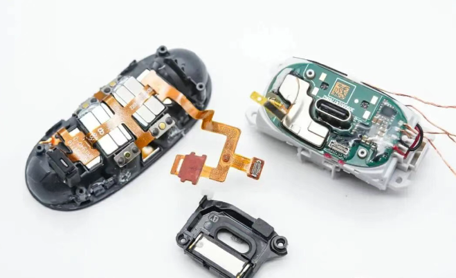
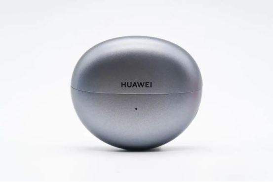
In the consumer electronics market, flagship products such as the HUAWEI FreeClip open-ear headphones demonstrate the industry’s increasing demand for compact, reliable, and high-precision components. Modern premium wearables push the limits of hardware integration, requiring components that offer both structural durability and microscopic footprints.
This case study analyzes the engineering and manufacturing challenges commonly found in premium wireless audio devices and illustrates how Goldconn’s precision manufacturing capabilities—encompassing custom Type-C connectors, micro-stamping, and insert molding—address these exact tier-1 industry requirements. By aligning production processes with these strict benchmarks, Goldconn helps original equipment manufacturers (OEMs) achieve seamless component integration, minimize assembly defects, and accelerate time-to-market.
1. The Challenge: High Component Density and Environmental Sealing in Premium Wearables
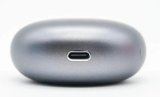
The compact, rounded architecture typical of modern wireless audio charging cases leaves minimal internal volume for hardware integration. Hardware engineers face severe spatial and environmental constraints when designing or sourcing external charging interfaces:
- High-Density Internal Layouts: Standard charging enclosures must simultaneously house high-capacity battery cells, wireless charging receiver coils, power management chipsets, and independent acoustic components for tracking functions. For product designers, this means the charging interface must feature an ultra-low vertical and horizontal footprint to avoid interfering with neighboring electronics.
- Mechanical Endurance Under High-Frequency Wear: As the primary point of daily physical interaction, an exposed interface must withstand thousands of plug-and-unplug cycles. OEMs require structural reinforcement to prevent physical degradation, contact resistance variation, and eventual port failure over the product’s lifespan.
- IP-Rated Environmental Protection: Premium wearables frequently require IP68 or higher dust and water resistance ratings to endure daily exposure to sweat and moisture. Because an external charging port represents a vulnerable entry point, the interface demands airtight structural sealing where the connector body meets the plastic housing to eliminate the risk of internal short circuits.
2. Engineering Solution: Micro-Precision Customization for Space Optimization
To address these typical design constraints, Goldconn develops custom component solutions engineered to optimize internal spatial efficiency while maintaining electrical reliability and assembly consistency:
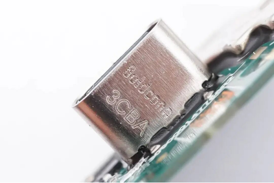
- Micro-Footprint Type-C Interfacing: Goldconn develops specialized Type-C female socket solutions featuring reduced shell dimensions and optimized pin spacing. This configuration allows OEM engineers to achieve space optimization, ensuring the connector sits perfectly flush on dense motherboards without disrupting the layout of adjacent power modules or acoustic tracking systems.
- Stamped Metal Protective Trims: To combat physical wear at the insertion point, Goldconn utilizes automated, tight-tolerance stamping to produce exact-fit metal protective rings. These structural accents shield the plastic edges of the device enclosure from frictional wear during cable insertion. This solution protects the cosmetic and functional integrity of the housing, reducing field return rates for OEMs.
- Airtight Insert Molding Solutions: To support IP-rated environmental requirements, Goldconn applies tight-tolerance insert molding processes that fuse metal connector shells with plastic structural housings. This eliminates microscopic gaps at the material boundaries, creating a reliable moisture barrier that protects active circuitry and enhances overall product durability.

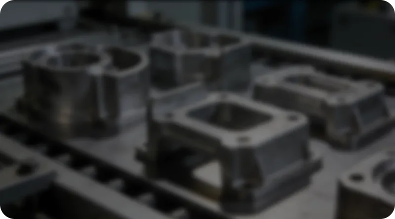
3. Manufacturing Capability: Delivering Quality and Consistency at Scale
Successfully addressing flagship-level engineering challenges relies on a manufacturing infrastructure capable of translating complex specifications into defect-free mass production:
- Automated Precision Stamping: Goldconn operates high-speed, automated stamping lines capable of producing micro-sized metal structural parts, shielding cans, and contact terminals with consistent tolerance controls. This high repeatability ensures that every batch integrates flawlessly into automated OEM pick-and-place assembly lines, maximizing production yields.
- Tight-Tolerance Injection Molding: By precisely managing mold temperatures and injection pressures, Goldconn ensures consistent material density around metal inserts. This eliminates structural warping and dimensional drift, providing procurement managers with predictable component fitting during final assembly.
- Certified Quality Management Systems: Goldconn’s production facilities operate under strict compliance with IATF 16149 (Automotive Grade) and ISO 9001 standards. Components undergo comprehensive environmental validation—including automated optical inspection (AOI), salt spray corrosion analysis, and mechanical endurance cycling—ensuring compliance with global technology brand auditing standards.
4. Validation and Manufacturing Result
Physical verification of high-density hardware assemblies confirms that utilizing precision-engineered connectors and stamped components ensures uniform solder alignment, stable retention force, and clean board placement inside tight retail housings. For B2B buyers, sourcing components manufactured to these rigorous tolerances results in reduced assembly-line downtime, optimized manufacturing yields, and a lower total cost of ownership.
5. Core Capabilities for Consumer and Industrial Electronics
Goldconn applies the manufacturing discipline required for high-end consumer technology across its primary production services. Hardware engineers and procurement professionals can leverage these core capabilities for their custom applications:
- Advanced Connector Manufacturing: Production of standard and customized 6-pin, 16-pin, and 24-pin Type-C interfaces, including vertical, mid-mount, sink-type, and waterproof configurations up to USB 4.0 specifications.
- Precision Metal Stamping & Tooling: Custom fabrication of micro-sized metal structural parts, contact terminals, custom brackets, and internal shielding components with strict tolerance alignment.
- IP-Rated Waterproof Engineering: Development of custom component housings and interface seals engineered specifically to meet IP67/IP68 dust and moisture protection standards in compact consumer, industrial, and automotive designs.
- Full-Scale Mass Production Scalability: Transition support from initial engineering validation testing (EVT) and design validation testing (DVT) through to high-volume automated production.
6. Conclusion
Flagship devices like the HUAWEI FreeClip highlight the industry’s shift toward absolute precision and rugged environmental sealing in ultra-compact form factors. Goldconn addresses these market needs by combining advanced engineering support with certified, repeatable manufacturing processes.
Whether you are designing next-generation wearable audio devices, rugged handheld industrial scanners, or high-density automotive electronics, Goldconn delivers the component reliability and assembly consistency your project demands.
Partner with Goldconn for Your Next Project Looking for a precision component manufacturing partner for your next consumer electronics project? Goldconn provides customized connector, stamping, and molding solutions from engineering validation to mass production.
[Contact Our Engineering Team Today] to request technical drawings, samples, or a detailed manufacturing quotation.