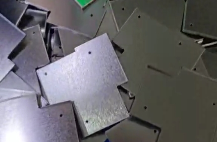
In modern electronics, high-speed signal processing and compact component layout make electromagnetic interference (EMI) a critical engineering challenge. Custom metal shielding covers (often referred to as EMI/RF shielding cans) provide the physical barrier necessary to isolate sensitive radio frequency (RF) sections, power management units, and processors.
Achieving consistent shielding effectiveness at volume requires uncompromising stamping precision. Here is a closer look at how high-quality shielding covers are manufactured at Goldconn, from precision die setup to automated mass production.
The Manufacturing Workflow: Engineering Repeatable Precision
- Material Selection & PreparationEMI shields typically utilize nickel silver (German silver), tin-plated cold-rolled steel (SPTE), stainless steel, or brass. Nickel silver and tin-plated steels are especially popular for their excellent solderability, corrosion resistance, and magnetic/dielectric attenuation performance without requiring secondary plating after forming.
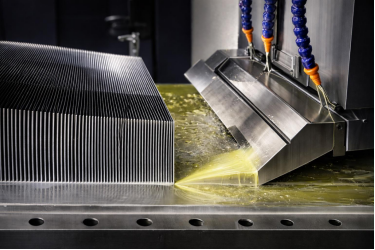
- Progressive Die Tooling & AlignmentAs shown in our production line, tooling accuracy is the foundation of tight-tolerance manufacturing. Using high-precision stamping dies fitted with durable guide pins and nitrogen/heavy-duty coil springs, the setup ensures zero lateral deviation across high-speed cycles.
- Multi-Stage Progressive Stamping & BlankingContinuous metal strip feeds into the press, undergoing progressive stations that punch positioning holes, dimples, edge notches, and fold tabs. The high-tonnage punch ensures clean shear edges and burr-free borders, which are essential for surface-mount technology (SMT) coplanarity.
- Automated Ejection & In-Line Quality ControlFormed shielding covers are rapidly blanked and ejected directly along low-friction guide chutes into automated collection bins. Throughout the run, critical dimensions—including wall flatness, solder-tab coplanarity (strictly controlled within $\pm0.05\text{ mm}$), and vent hole positions—are verified using optical coordinate measuring systems to eliminate PCB soldering issues.
Key Product Highlights & Engineering Advantages
- High Shielding Effectiveness (SE): Seamless perimeter design and optimized vent apertures balance thermal dissipation with broadband EMI/RFI attenuation.
- Superior SMT Solderability: Uniform surface finish guarantees reliable reflow soldering directly onto PCB ground traces or clip-in spring fingers.
- Tight Coplanarity Tolerances: Eliminates pseudo-soldering and tombstoning risks during automated high-speed SMT assembly.
- Rapid Prototyping to High-Volume Scale: Backed by in-house tooling design and IATF 16949 / ISO 9001 certified quality management.
Typical Application Scenarios
- Telecommunications & Networking: 5G base station modules, optical transceivers, Wi-Fi 6/7 routers, and RF power amplifiers.
- Automotive Electronics: ADAS radar systems, infotainment head units, and EV battery management systems (BMS).
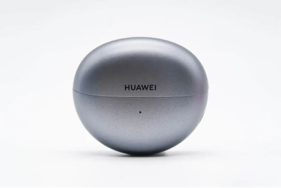
- Consumer & Smart Devices: Smartphones, IoT gateway modules, smart wearables, and POS terminals.
- Industrial & Medical Equipment: Precision instrumentation, diagnostic sensors, and robotics controllers where noise isolation is critical.
Partner with Goldconn for Your Custom EMI Shielding Needs
Whether you require a one-piece fixed frame or a two-piece snap-on shield cover for easy board rework, Goldconn delivers end-to-end tooling, stamping, and DFM support to accelerate your product development cycle.
Ready to optimize your board-level shielding design?
Contact our engineering team or explore our custom metal fabrication capabilities at Goldconn Official Website.